Description
We are the Singxer USA distributor! Shipped from USA!
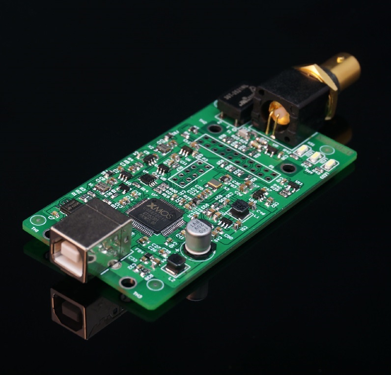
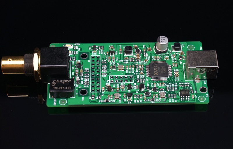
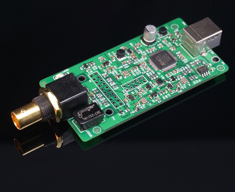
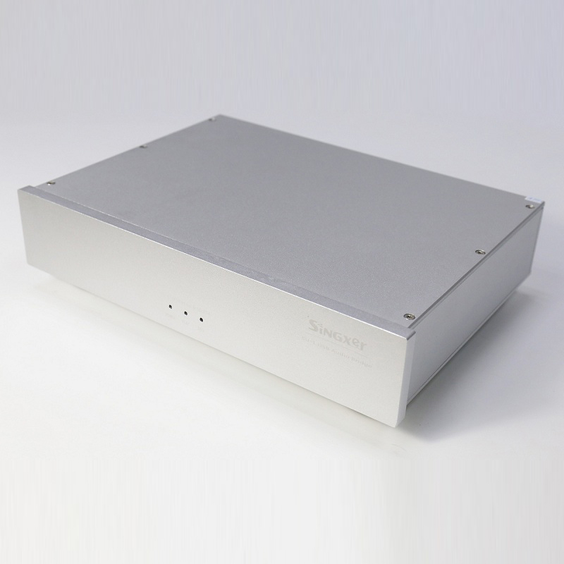
X-1 digital interface module xCORE-200 interface full network starting latest XMOS, the first use of the second generation XMOS chip XU208 developed USB interface, but also the first to support firmware upgrade interface .
Product Description:
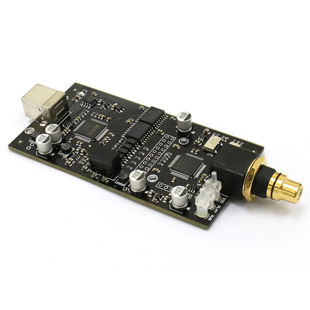
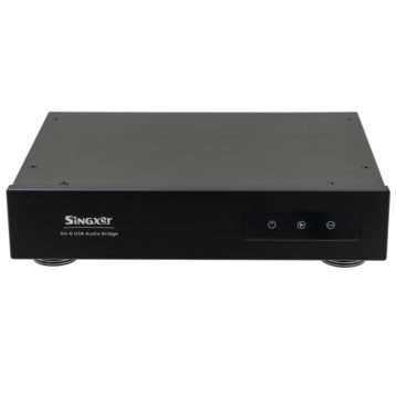
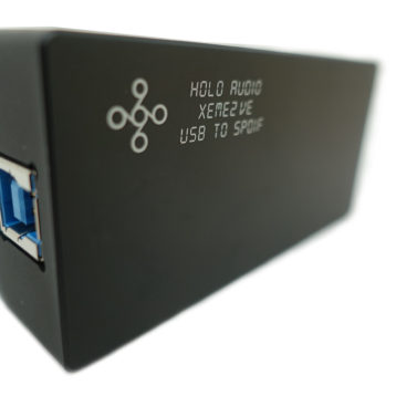
X-1 digital interface of our team to develop a high-performance USB digital audio interface, using the XMOS latest xCORE-200 series chips. X-1 is the rare Japanese KDS low jitter TCXO clock digital system interface. X-1 digital interface using standard USB2.0 input interface, while X-1 has a wealth of output interfaces, including coaxial RCA and I2S interfaces.
Features:
1, X-1 is the first using the XMOS latest xCORE-200 series USB digital interface products. New generation XMOS chip, using more advanced process technology, performance than the older U8 chip doubled, reaching 1000MIPS processing capabilities.
2 , it is known, the weight of the core is digital audio algorithms. Our team in the field of digital audio work for many years, at the same time get XMOS FAE support team, we conducted a number of technical improvements and optimization algorithms on the basis of the original firmware.
Each interface electrical standards:
1 , the USB input socket is a standard USB-B type female, the USB power supply range 4.5V-5.1V ;
2 , the RCA connector outputs standard S / PDIF signal level is 550mV ( access standard load ), the output impedance of 75 ohms;
Design details:
1 , carry out electricity as the mother of the acoustic design concept, pay attention to the power supply circuit design, high-performance, low noise and fast response of the LDO as the main power source. The entire board using 2 independent way of LDO power supply, wherein the clock even partially adopted ADI ‘s ultra low noise LDO , in order to ensure the ultimate output performance laid a solid foundation.
2 , the PCB motherboard with 4 -layer circuit board design, ensure that you have full power and ground plane layer, using the method of high-speed digital design, signal integrity and power integrity of the entire board. The clock signal for special treatment, using package design and precise impedance control, thereby ensuring the signal quality and increase the clock anti-jamming capability. Input and output signals follow a standard design, especially USB high speed signals using a 90 ohm differential impedance control.
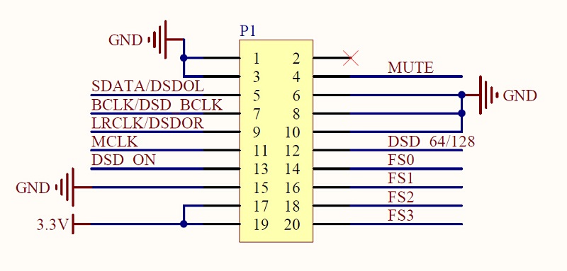
Here is the I2S pin pin descriptions, please note that when using the pin order.
FS0, FS1, FS2 frequency indication in the table below:
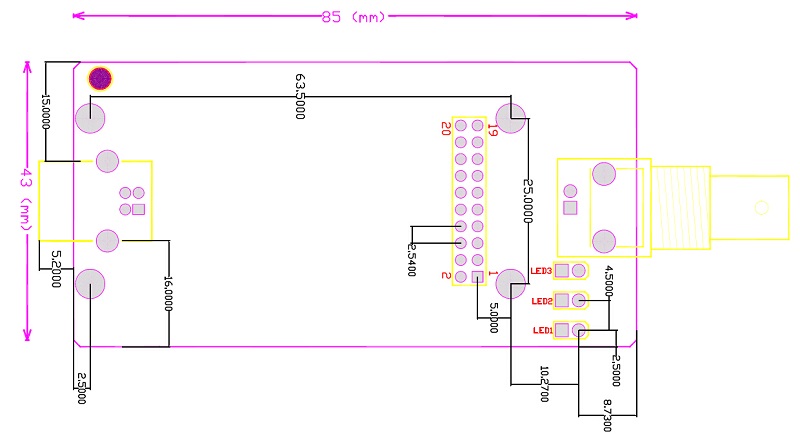
Schematic diagram of the following boards, and pin numbers.
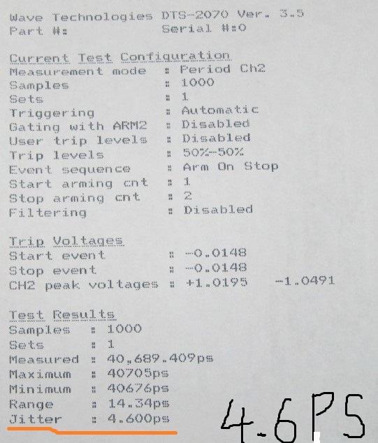
Here is the jitter test parameters: You can see jitter as low as 4.6PS







Reviews
There are no reviews yet.