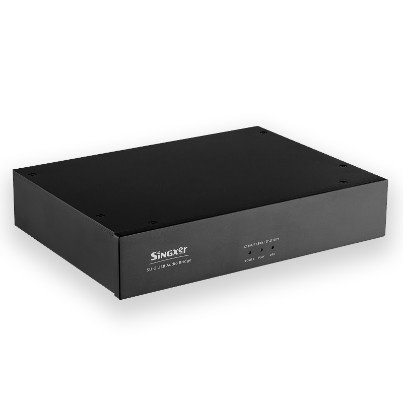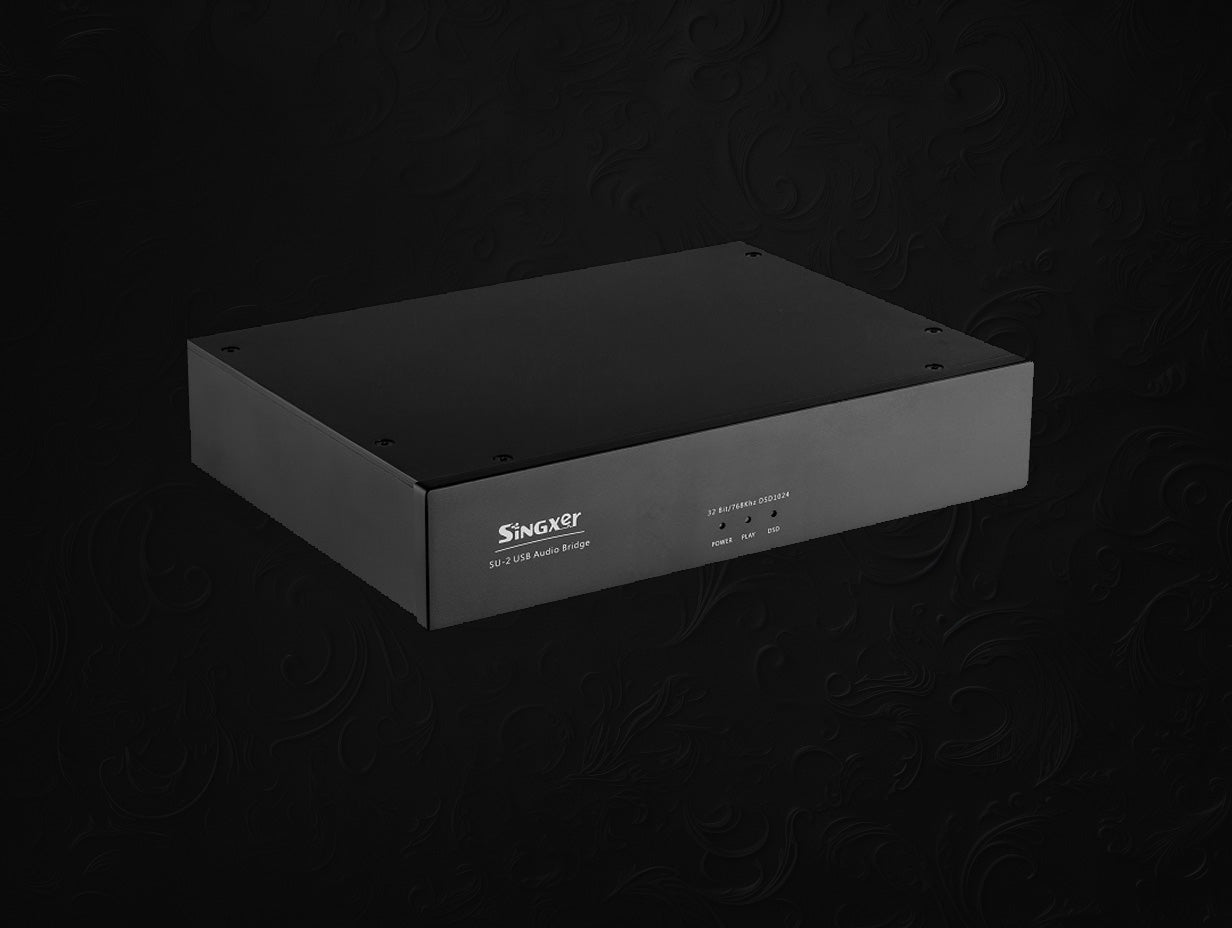
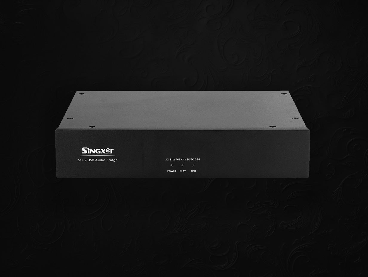
Singxer SU-2 – DSD1024 USB Digital Interface Femto second clock Interface – PCM 768k, HDMi i2s DDC, ARM Processor

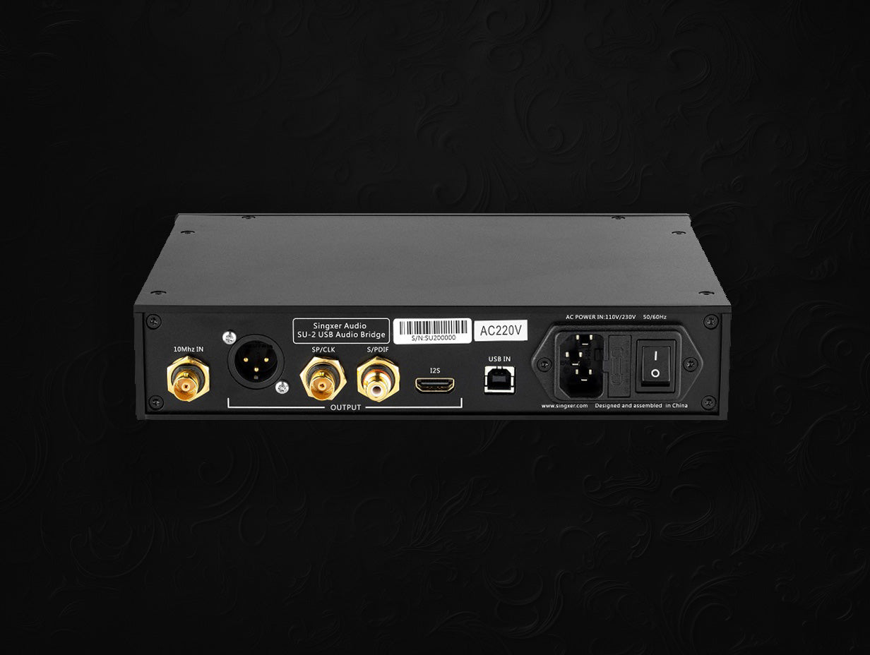
Description
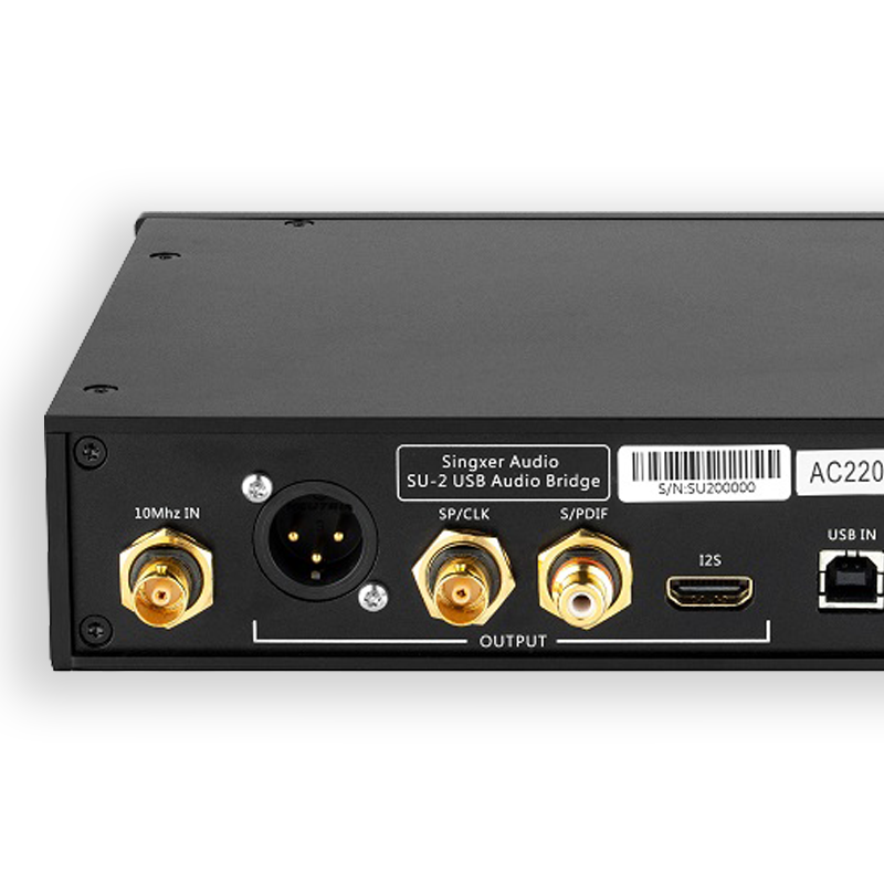
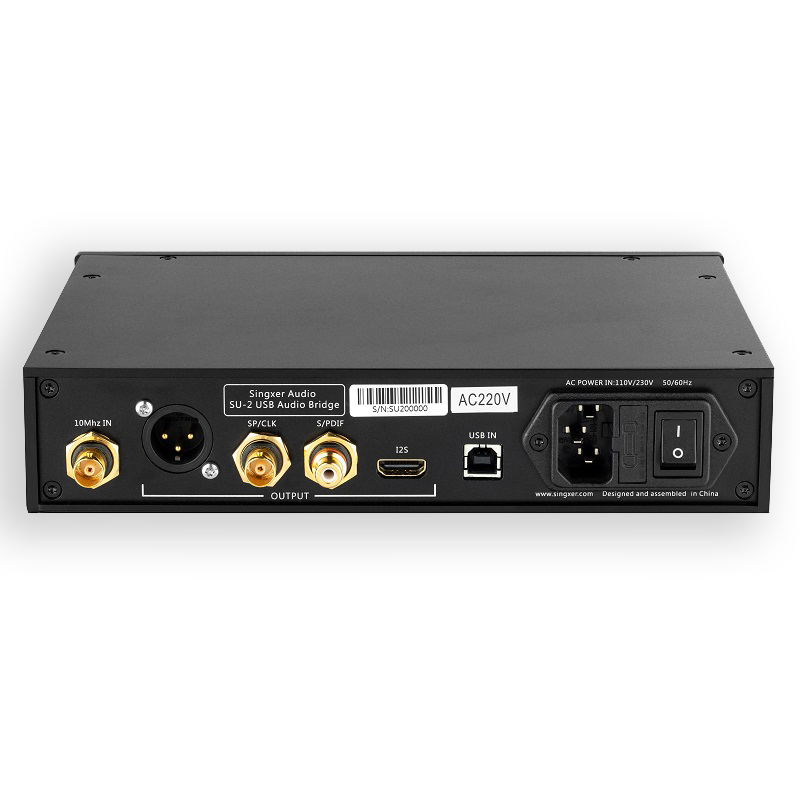
The SU-2 is not only a USB interface, it can also be used as an independent master clock product.
1. When used as an independent master clock, it can output a word clock of 44.1K-384K, or output a master clock of 22.5792Mhz-49.152Mhz. (When not connected to USB, it will be used as the master clock device by default)
2. When using an external 10Mhz clock input, it can also be used as a frequency converter; support 10Mhz to 44.1K-384K word clock, or output 22.5792Mhz-49.152Mhz master clock.
SU-2 is a new architecture USB interface developed by us to replace the original SU-1; PCM sampling rate supports up to PCM 768K, and DSD supports up to DSD1024. Using a large FPGA as the core of the processing processing, we decentralized some of the FPGA algorithm technology of the flagship interface SU-6 to the SU-2; its positioning in the mid-to-high-end interface mainly uses the following three unique technologies:
1. Full isolation technology (ground isolation), using 150Mbps full isolation chip, can completely isolate the interference from the PC;
2. Source synchronization technology and FPGA shaping technology, reshape the I2S signal after isolation; thus eliminating the additive jitter brought by the isolation chip;
3. Self-developed clock system, using ACCUSILICON high-performance crystal oscillator, low phase noise, low jitter; you can also choose external 10Mhz clock, support various atomic clocks, constant temperature crystal, GPDSO input.
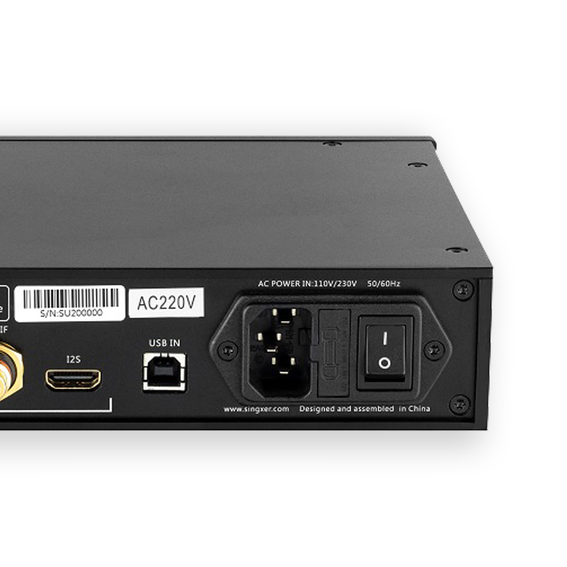
This product supports two kinds of AC power voltage, 230V and 115V respectively. Please choose the volts suitable for your country’s voltage.
The driver was updated in June 2019. The latest version is V4.67. The latest driver supports DSD1024 and DSD NATIVE modes.
We attach great importance to the design of power supply circuits, using LDOs with high performance, low noise and fast response as the main power supply. The entire board uses multiple independent LDO power supplies, and the clock part even uses ADI’s ultra-low noise LDO, which lays a solid foundation for ensuring the ultimate output performance. (KTE SU2 has vastly improved discrete voltage regulators)
The PCB main board adopts a 4-layer circuit board design to ensure a complete ground plane and power layer. A high-speed digital design method is used to ensure the signal integrity and power integrity of the entire board. The clock signal is specially processed, and the grounded design and precise impedance control are adopted to ensure the clock signal quality and improve its anti-interference ability. The input and output signals follow the standard design, especially the USB high-speed signals use 90 ohm differential impedance control.